
要点
- On 9 November 2026, Amin Vahdat announced TPU 8tx and TPU 8i Max, expanding Google's eighth-generation TPU portfolio to four systems in a single year, which the post calls a first.
- Google draws a distinction in the post itself: a new chip is a multi-year silicon project, while a new system is how compute, networking, and storage are packaged around a chip that already exists.
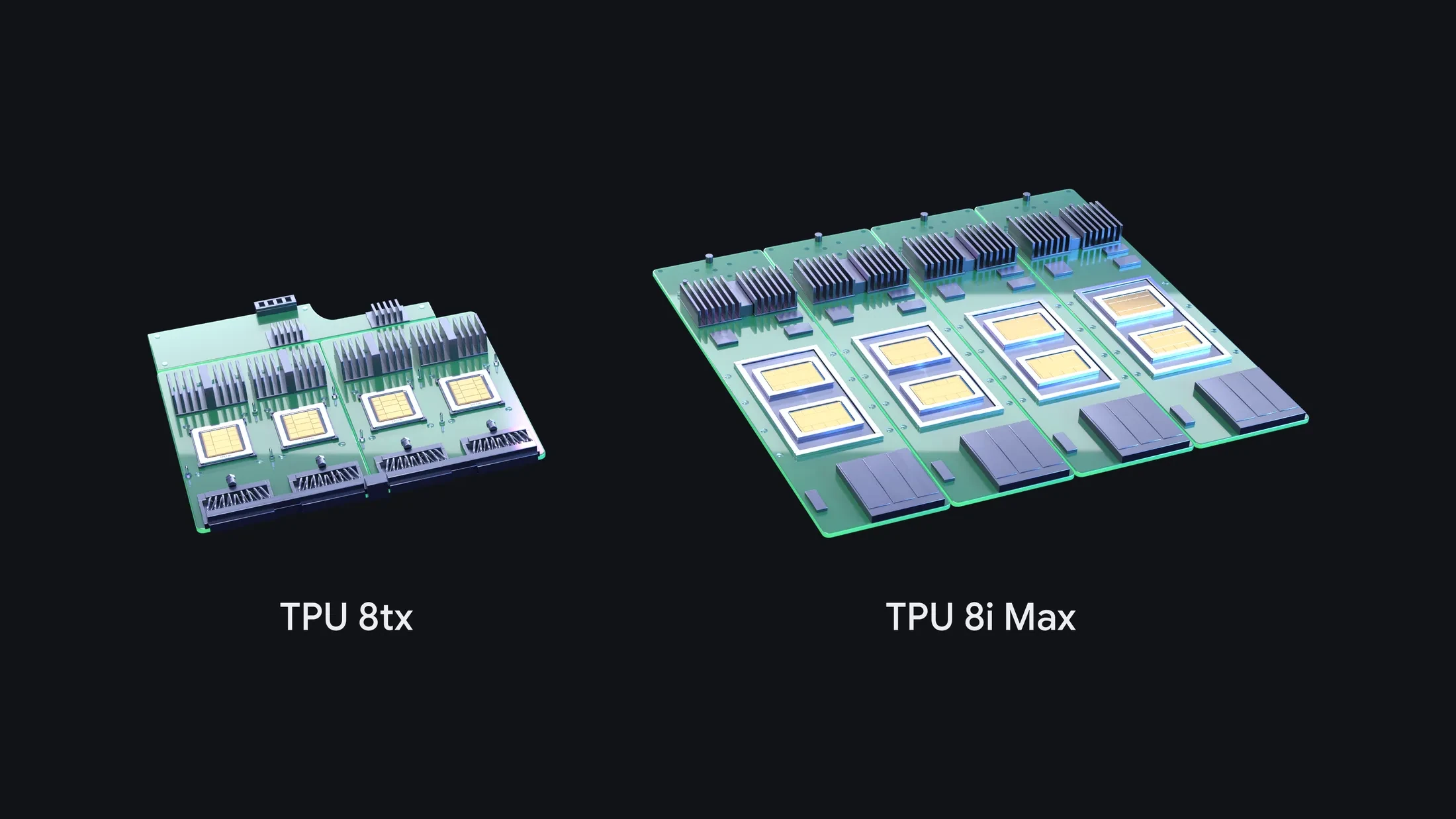
- TPU 8tx is built for confidential inference and small-scale training. It keeps data and model weights isolated even while in use, is paired with 5th Generation AMD EPYC CPU hosts, and is said to deliver up to 2x lower latency than TPU 8t with a near-zero performance penalty.
- TPU 8i Max puts two TPU 8i chips in one package, doubling compute, on-chip SRAM, and HBM bandwidth (the high-bandwidth memory next to the chip) inside the existing rack footprint.
- The same post announces software, including open-source TorchTPU, TPU Sync (said to cut KV-transfer latency and time-to-first-token by more than 90%), Cloud Pathways now generally available, and GKE dynamic slicing (up to 5x faster job startup and 4.5x faster fault recovery).
On 9 November 2026, Amin Vahdat, writing on Google's blog, announced two additions to the company's eighth-generation TPU line: TPU 8tx, aimed at confidential inference, and TPU 8i Max, aimed at large context windows and more compute in the same rack. This is the first year, the post says, in which Google has introduced four TPU systems. The sentence that should govern the reading is Google's own. A new chip means laying out a new piece of silicon, a process measured in years. A new system means changing the package, the memory, the network, and the software around a chip that is already in hand. 8tx and 8i Max are presented as the second kind.
[1]Chip versus system
Google first described TPU 8t and TPU 8i at Cloud Next in April. 8t was the training system. 8i was the reasoning system, designed, the earlier claim said, to cut inter-chip communication delays by up to half. Those two chips, the April figures said, offered up to 2.7 times better training performance and 80% better inference price-performance than the previous generation. Today's post adds two configurations of that same generation.
TPU 8tx uses the same silicon as TPU 8t, paired with 5th Generation AMD EPYC CPU hosts. Its selling point is confidential compute: data is usually encrypted at rest and on the network, but has to be unlocked in memory while a computer works on it. 8tx, Google says, keeps sensitive data and model weights protected and isolated even while they are in use. It also adopts the low-latency Boardfly network created for real-time reasoning, and is said to deliver up to 2x lower latency than TPU 8t, with a near-zero performance penalty. Because it pairs training-grade compute with a fast inference network, the post says a team can fine-tune a model on private data, distill a large model into a smaller one, and train agents with reinforcement learning, without moving that data between separate clusters.
TPU 8i Max is a packaging change of a different kind. Google took two low-latency TPU 8i chips and put them on a single package. The result, it says, is double the compute, double the SRAM, and double the HBM bandwidth of TPU 8i, so large jobs are less likely to stall when many agents work across a codebase or hours of video. Because twice the silicon fits in the existing rack footprint, the post argues that a data center can put more computing power in the same floor space and the same power budget.
The four-system lineup is then assigned roles: 8t for scale-up training, 8i for low-latency reasoning, 8tx for confidential computing, and 8i Max for massive context windows and the highest compute density per rack. Google also says TPUs now serve nearly 100 customers, including frontier labs, trading firms, retailers, and universities, and that some customers can deploy TPUs in their own data centers.
[1]The software that arrives with the hardware
A large share of the post is not about the two new systems at all. It is about making TPUs easier to use, and about software that tries to keep expensive chips from sitting idle.
Last month Google open-sourced TorchTPU, so PyTorch code and Hugging Face models can run on TPUs without a rewrite, with TPU backends for vLLM and SGLang. A TPU agent suite, now in preview, is meant to plug into coding tools such as Claude Code, Cursor, and Google Antigravity to help with onboarding, bottleneck diagnosis, and kernel tuning in plain language. An open-source XLA Serving Engine is described as a way to train in Python and serve in a low-latency C++ runtime across TPUs, GPUs, and CPUs.
On production benches, the post points to InferenceX and AgentX results published by SemiAnalysis, and says a native vLLM-TorchTPU stack on TPUs reached state-of-the-art price-performance marks on those tests of agentic coding and long-context work. Those citations are third-party price-performance results on named benchmarks. They are not, in the text, a general claim that TPUs beat every rival accelerator on every job.
Other software claims are more operational. An Agent Compute Engine is said to suspend and resume idle agent sessions, so a chip is not left running while a job waits on a database, a tool, or a person. TPU Sync, a model-state layer now being open-sourced, is said to move large KV caches (the model's working memory of what it has already processed) off the chip in milliseconds, and to cut KV-transfer latency and time-to-first-token, the wait before the first piece of output appears, by more than 90%. Cloud Pathways, the DeepMind runtime behind Gemini, is now generally available on Google Kubernetes Engine, with a single controller for large TPU systems. GKE dynamic slicing, also now generally available, uses optical circuit switching to assemble or split TPU cubes on the fly, and is said to cut job startup times by up to 5x and fault recovery by up to 4.5x.
[1]The fair case, and what is missing
The fair reading is the one Google is inviting: when software needs change faster than a new chip can be designed, the useful move is to re-package silicon you already have. Confidential compute for regulated customers, and more memory bandwidth in the same rack for long-context agents, are both requests that do not have to wait for a ninth generation. The post is unusually plain about that distinction.
The numbers still need to be read as vendor "up to" figures, unless a third party has already measured them. The 2x latency claim, the near-zero penalty, the doubled bandwidth, the 90% cut in time-to-first-token, and the 5x and 4.5x cluster figures are Google's. The SemiAnalysis citations can be checked, but this post does not reprint the full method or the rival configurations. There is no datasheet in the article for clock rates, memory capacity, or list prices of 8tx and 8i Max. "Nearly 100 customers" is a business figure, not a utilization or performance result.
[1]Who should care, and what to watch
Cloud customers who have been waiting for confidential inference on TPUs, and teams whose agents are stalling on long context, should care. So should anyone comparing a "new TPU" headline with a new NVIDIA or AMD chip announcement. These are not the same kind of launch.
In the next six months, the checks are whether 8tx is actually used for private fine-tuning in regulated settings, whether 8i Max's density claim shows up in deployed racks, and whether PyTorch-on-TPU and the SemiAnalysis price-performance results still hold once more outside teams run the same benches.
[1]Close
Google's own frame is the right one. 8tx and 8i Max are systems built around eighth-generation chips to meet two requests the April machines did not fully cover: data that must stay protected while it is being used, and more memory bandwidth in the same footprint. The hardware claims will be settled by deployments and by those third-party benches, not by the phrase "agentic era."
[1]